FPGA 中的延时
Posted on 2014-11-23 14:03 in IC
Delay in circuits
从模拟电路的知识,我们可以知道 电路中存在很多类型不同的延时。 比如:
-
propagation delay
我们通常假设信号在电平之间变化时瞬间完成的,但是实际情况并不是瞬间完成,电路需要花费一段时间才能完成电平的转化。晶体管的开关特性对于不同的变化有不同的表现:
-
上升延时 (
rising delay),输出变为 1 -
下降延时 (
falling delay),输出变为 0 -
关闭延时 (
turn-off delay),输出变为高阻 Z -
输出变为 X 的时延
原因就是(Digital Design (Verilog): An Embedded Systems Approach Using Verilog):
One factor that causes signal changes to occur over a nonzero time interval is the fact that the switches in the output stage of a digital component, illustrated in Figure 1.15, do not open or close instantaneously. Rather, their resistance changes between near zero and a very large value over some time interval. However, a more significant factor, especially in CMOS circuits, is the fact that logic gates have a significant amount of capacitance at each input.
这个答案也解释了为什么在设计中要避免大扇出信号:因为大扇出意味着输出端并联着很多电容,电容负载较大时造成连接信号转换相对较慢的原因。
The total capacitive load is thus the sum of the individual capacitive loads. The effect is to make transitions on the connecting signal correspondingly slower. For CMOS components, this effect is much more significant than the static load of component inputs.
我们可以把对晶体管的讨论推广到其他的数字元件:
A similar argument regarding time taken to switch transistors on and off and to charge and discharge capacitance also applies within a digital component. Without going into the details of a component’s circuit, we can summarize the argument by saying that, due to the switching time of the internal transistors, it takes some time for a change of logic level at an input to cause a corresponding change at the output. We call that time the
propagation delay, denoted bytpd, of the component. -
-
wire delay
另外一种延时是信号在导线上传播时产生的延时,一般我们都把这种延时假设也 0,也就是说导线时理想的导体,信号经由导线的传输没有任何延迟。如果导线很短,或者芯片上不超过 1mm 的导线来说,这种假设是合理的。但是当设计高速电路时,不能忽略这种导线存在的寄生电容和电感,这时候导线应该被视为传输线,必须精心设计。
至于如何设计应该属于模拟电路的部分,这里不讨论。
关于上面的两种延时,FPGA-Based System Design 里面有详细讨论如何建模、如何计算具体时延的值。
即使对于同一种信号跳变,延时也分为不同的类型:
-
最小值 (
minimum) -
典型值 (
typical) -
最大值 (
maximum)
Models in Verilog HDL
为了对电路中的时延现象进行建模,Verilog HDL 定义了延时语法。
-
对于上升、下降、关闭时延,可以使用逗号按照顺序将三者分开:
1
2
assign #(1, 2) A-xor-wire = eq0 ^ eq1;
assign #(1, 2, 3) A-xor-wire = eq0 ^ eq1;
第一句表示一个异或门上升时延为 1,下降时延为 2,关闭和 X 时延为两者中的最小值,即 1;
第二句表示一个异或门的上升、下降、关闭时延分别是 1,2,3,X 时延为 3 者中的最小值,即 1。
-
对于最小值、典型值、最大值可以使用分号按照 min:typ:max 的顺序,将 3 者分开:
1assgin #(2:3:4, 3:4:5) A-xor-wire = eq0 ^ eq1;表示上升时延的 min:typ:max = 2:3:4,下降时延的 min:typ:max = 3:4:5。
需要注意到一点是,当延时出现在 wire 信号的定义处时,会和普通的赋值语句中的延时稍有不同。
1 | |
这个叫做 net delay,它是和 wireA 绑定的,对 wireA 进行的任何赋值必须延迟 10 个时间单位之后才有效。当在连续赋值语句中,延时是属于连续赋值语句的一部分,而不属于 net,所以只在这一句中有效,对其他赋值语句没有影响。
一般来说,assign 语句中的延时特性会被综合工具忽略。因为综合工具需要完成的功能就是将代码描述映射为逻辑电路,而逻辑电路中的延时是由最基本的单元库和走线延时决定的,用户是无法对逻辑单元指定延时长度的,只能在综合、实现时添加时序约束条件,使工具尽量满足要求。
Implement
Verilog HDL 中的延时语法不可综合并不代表就不能在实际电路中实现延时。
在实际电路中,不同的情况下需要采用不同的方法来实现延时:一般来说,异步电路的时延通过门延时来完成,比较难预测,而同步电路的时延通过触发器或者计数器来实现。
in ASICs
在早期的逻辑电路图设计阶段,有且设计者养成了手工加入 Buffer 或者非门调整数据 延时的习惯,以保证本级模块的时钟对上级模块数据的建立及保持时间的要求。这些做法目 前主要应用于两种场合:
-
分离电路
使用分立逻辑单元(如 74 系列)搭建数字电路一般为复杂度比较低、系统灵活性比较低的场合。使用分立元件时,由于可以使用的元件比较少,而且一般设计频率比较低,时序裕量比较大,所以采用 Buffer、非门等单元来调整时延时可以接受的。
-
ASIC 领域
在 ASIC 中采用这种方法,是以严格的仿真和时序约束为前提的。
in FPGAs
在 ASIC 中采用的添加 Buffer、非门的设计方法并不适合 FPGA/CPLD 等可编程逻辑,在 FPGA 中应该尽量避免这种设计。
The Art of Hardware Architecture:
Delay chains occur when two or more consecutive nodes with a single fan-in and a single fan-out are used to cause delay. Often inverters are chained together to add delay. Delay chains generally result from asynchronous design practices, and are sometimes used to resolve race conditions created by other combinational logic. In both FPGA and ASIC, delays can change with each place-and-route. Delay chains can cause various design problems, including an increase in a design’s sensitivity to operating conditions, a decrease in a design’s reliability, and difficulties when migrating to different device architecture. Avoid using delay chains in a design, rely on synchronous practices instead.
总结下来主要就是 3 个原因:
-
设计的可靠度低
Buffer、非门都是组合逻辑,组合逻辑最大的问题就是容易出现毛刺,电路可靠度不高,这种方法的时序裕量小,对环境敏感(特别是温度),一旦外界环境发生变化,时序可能就会完全紊乱、导致电路瘫痪。
-
设计的移植难度大
一旦芯片换代,或者需要将设计移植到不同的器件上时,就必须对延时进行重新调整,电路的可维护性和扩展性差。
-
信号通过多级非门时,综合器可能会将其优化掉。
虽然可以在代码中添加约束,防止综合器将其优化掉,但是不推荐这种方法,理由见前两条。
Xilinx FPGA 高级设计及应用 介绍了 FPGA 中应该采用的方法:
-
专门的延时器件
在 FPGA/CPLD 内部延时电路结构由一种标准的宏单元描述。虽然各家芯片的宏单元描述不同,但总的来说都是 一些逻辑 + 一个 / 两个触发器构成。
Altera FPGA 中可以对信号加一个或多个 LCELL 来产生一个延时。(Xilinx 的没有查到 ...)
虽然厂家提供了延时单元,但是这种延时并不稳定,会随着外界环境(比如温度)的变化而变化,所以并不提倡这种方法。
网上有人讨论这种方法的应用:fpga 内部的延时单元
-
触发器 or 计数器
如果延时相对较小,可以使用高频时钟来驱动一个移位寄存器,将待延时的信号当作输入,按照需要的延时来设置移位寄存器的级数,最后的输出即延时的结果。
如果延时相对较大,可以使用计数器来延时输出。
====================== Update 01/31/2015 ========================
Simulation
我们知道,仿真器使用 “ 事件 ” (event) 来模拟实际的电路行为,但是毕竟软件和硬件还是不同的,而 Verilog 语言又是很灵活的,如果不加注意,很可能不能对电路进行正确的建模。Clifford E. Cummings 大神写了一篇 paper 介绍了 Verilog HDL 中应该如何正确使用延时,才能保证建模的正确性:
Correct Methods For Adding Delays To Verilog Behavioral Models
下面我的笔记,摘录一部分内容和结论:
要讨论正确的延时的代码风格,首先要了解仿真器在对延时进行建模时,通常使用的两种不同类型的 Delay 模型:
-
Inertial delay模型 惯性时延,专门描述一些特殊信号传播到输出端口所耗费的时延,这部分信号特殊在于:输入信号必须保持稳定一段时间(等于或大于传播时延)。如果输入信号的变化时间间隔小于过程赋值延时 / 连续赋值延时 / 门延时(也就是说在计算出一个结果并且还没有来得及输出,输入信号又发生了变化),那么前一时刻值的旧事件会被新值的事件代替,重新触发计算,并输出。 -
Transport delay模型传播时延,用来描述当任何一个输入信号一旦发生变化后,所有信号到输出的延时。所有的输出变化值会按照顺序排队输出。
有了上面两个延时的概念之后,我们就可以分类讨论下面三种情况下应该如何添加延时了。
Blocking assignment
在阻塞赋值中,通常添加延时的方法有两种:
-
left-hand-side
1#5 y = ~a; -
right-hand-side
1y = #5 ~a;
但是这两种方法都有可能存在问题:
以描述一个输出延迟为 12ns 的加法器,如果我们在左边添加延时,
1 2 | |
在下图时序中可以看到,当 t = 15 时,a 发生变化,触发 always 块,模块计算新的求和结果。但是,在接下来的 t = 15 ~ 24 内,a、b、ci 分别发生了变化,所以当从触发开始,到 12ns 过后该输出结果时,计算结果的值使用的是当前最新的值(可以看到,ci 的变化和输出之间仅仅有 3ns < 12ns),而非触发时刻的值。
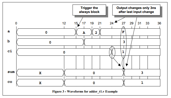
事实上,在任何阻塞赋值的左边添加延时都会存在类似的问题。
Modeling Guideline: do not place delays on the LHS of blocking assignments to model combinational logic. This is a bad coding style.
Testbench Guideline: placing delays on the LHS of blocking assignments in a testbench is reasonable since the delay is just being used to time-space sequential input stimuls events.
如果我们在右边添加延时,同样也会有问题。
1 2 | |
假设在 t = 15 时刻,a 发生变化,触发 always 块,模块会对当前的值进行采样,并且在 12ns 之后将采样结果输出,而在这 12ns 期间,输入端的任何变化都会被忽略,这意味着错误的旧值会一直保持下去,直到有新的变化重新触发。
Modeling Guideline: do not place delays on the RHS of blocking assignments to model combinational logic. This is a bad coding style.
Testbench Guideline: do not place delays on the RHS of blocking assignments in a testbench.
General Guideline: placing a delay on the RHS of any blocking assignment is both confusing and a poor coding style. This Verilog coding practice should be avoided.
Non-blocking assignment
在非阻塞赋值中,同样有两种方法来添加延时:
-
left-hand-side
1#5 y <= ~a; -
right-hand-side
1y <= #5 ~a;
仍然使用上面加法器的例子,如果我们在左边添加延时,会和阻塞赋值存在一样的问题:
1 2 | |
当 t = 15 时,触发 always 块,但是输出时结果时,使用的是最新时刻的值。
事实上,在任何非阻塞赋值的左边添加延时都会存在类似的问题。
Modeling Guideline: do not place delays on the LHS of nonblocking assignments to model combinational logic. This is a bad coding style.
Testbench Guideline: nonblocking assignments are less efficient to simulate than blocking assignments; therefore, in general, placing delays on the LHS of nonblocking assignments for either modeling or testbench generation is discouraged.
在非阻塞赋值的右边添加延时,会准确地描述前面介绍的 transport delays:
1 2 | |
当 t = 15 时刻,a 发生变化触发 always 块,此时会立刻对输入进行采样,然后等待 12ns 之后输出;在将这一时间存放在时间队列之后,always 块会被下一个变化时间重新触发,这意味着输出会随着输入的变化在 12ns 之后变化,如下图所示:
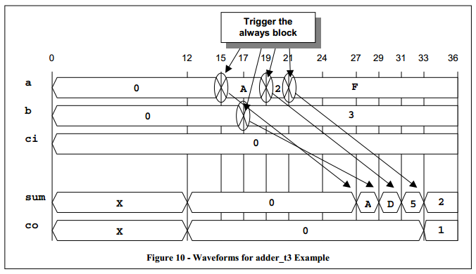
Recommended Application: Use this coding style to model behavioral delay-line logic.
Modeling Guideline: place delays on the RHS of nonblocking assignments only when trying to model transport output-prapagation behavior. This coding style will accurately model delay lines and combinational logic with pure
transport delays; however, this coding style generally causes slower simulations.Testbench Guideline: This coding style is ofen used in testbenches when stimulus must be scheduled on future clock edges or after a set delay, while not blocking the assignment of subsequent stimulus events in the same procedural blocks,
Modeling Guideline: in general, do not place delays on the RHS of nonblocking assignments to model combinational logic. This coding style can be confusing and is not very simulation efficient. It is a common and sometimes useful practice to palce delays n the RHS of nonblocking assignments to model clock-to-output behavior on sequential logic.
Testbench Guideline: there are some multi-clock design verification suites that benefit from using multiple nonblocking assignments with RHS delays; however, this coding style can be confusing, therefore placing delays on the RHS of nonblocking assignments in testbenches is not generally recommended.
Continuous assignment
连续赋值语句中,只能在左侧添加延时,在右边添加延时是非法的:
1 | |
在连续赋值语句的左边添加延时,会准确描述惯性延时(inertial delay),一般推荐使用这种方式。
以上面的加法器为例:
1 | |
如下图,在 t = 15 时刻,a 发生变化触发 assign 语句,应该在 t = 27 时刻输出结果,但是在 t = 17, 19, 21 时刻,a,b 分别发生了变化,这会导致有 3 个新的值,最终会只输出最后一个值(在 t = 21 + 12 = 33 时刻)。
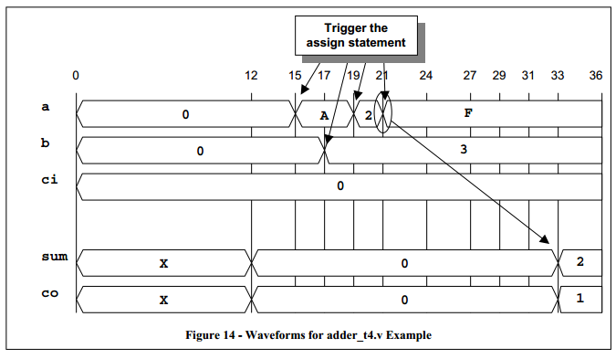
因为连续赋值语句不会排队输出这个概念,它只会跟踪输出结果,所以,连续赋值语句中的延时是对惯性延时(inertial delay)的建模。
混合方式:无延时的 always 块 + 连续赋值语句
1 2 3 4 | |
仍然会准确描述组合逻辑中的 inertial delay。在每个输入变化时,tmp 的值都会改变,在 tmp 改变的 12ns 之后,连续赋值的输出发生变化。tmp 一旦发生变化,assign 会重新赋值,重新延时,所以这种方式会准确描述组合逻辑的 inertial delay。
Modeling Guide: Use continuous assignments with delays to model simple combinational logic. This coding style will accurately model combinational logic with inertial delays.
Modeling Guide: Use always blocks with no delays to model complex combinational logic that are more easily rendered sing Verilog behavroral constructs such as "case-casez-casex", "if-else", etc. The outputs from the no-delay always blocks can be driven into continuous assignments to apply behavioral delays to the models. This coding style will accurately model complex combinational logic with inertial delays.
Testbench Guideline: Continuous assignments can be used anywhere in a testbench to drive stimulus values onto input port and bi-directional port and bi-directional ports of instantiated models.
Conclusions
always 块中的任何延时都无法准确对真实硬件的行为进行准确建模,应该避免这种延时建模。有一个例外:在非阻塞复制的右边添加延时,来描述 transport delay,但是这种方式是以仿真性能的下降为代价的。
在 连续赋值语句 / 无延时的 always + 连续赋值语句 中添加延时,这两种方式都会对 inertial delays 建模,推荐使用这种方式来对组合逻辑建模。
Reference
Digital Design (Verilog): An Embedded Systems Approach Using Verilog
The Art of Hardware Architecture: Design Methods and Techniques for Digital Circuits